![[back]](http://cs-www.uchicago.edu/images/logos/UofCsealTiny.gif) Department of Computer Science
The University of Chicago
Department of Computer Science
The University of Chicago
Last modified: Sun Jan 4 21:10:42 CST
In this lecture, we'll run through the essential structure of an electronic computer very briefly, observing how it can be implemented as a very large and carefully organized Boolean circuit.
Conventionally, electronic computers are understood in terms of 4 components:
We'll probe into the circuitry of the memory and processor just enough to get a rough idea of how it can all work.
Mention edge-triggered clocking vs. 2-phase clocking.
In principle, the same logical structure works for registers, which are memory elements in the processor, cache, and RAM memory. The individual bits are remembered by flip-flops, or by capacitors that can store a charge long enough for it to be read and refreshed. The interesting part is the addressing circuitry.
The height of a memory is the number of addresses. The width is the number of bits per address. The essential problem is to create a sufficiently high memory, 1 bit wide. A 1-bit wide memory is called a ``bitplane.'' By fanning out the address signal to a sequence of bitplanes, we can get as wide a memory as we like.
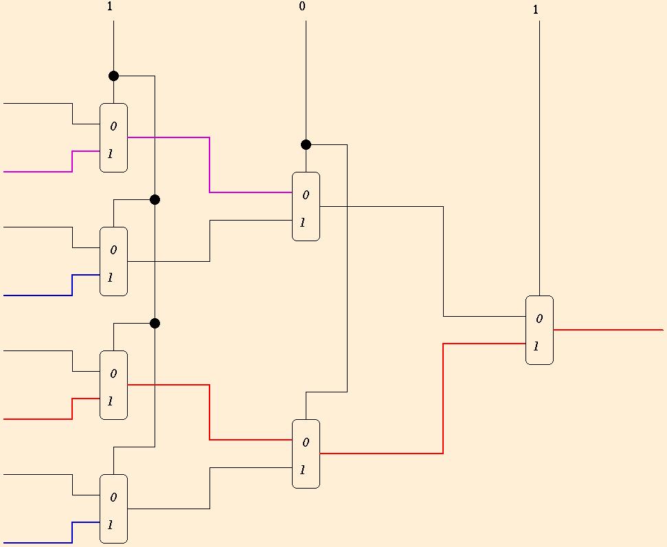
A multiplexor takes a 1-bit address, and selects one of two 1-bit
values. Two flip-flops plus a multiplexor is the read side of a memory
unit with 2 addresses each storing 1 bit. To get more addresses,
cascade multiplexors in a binary tree as shown below:
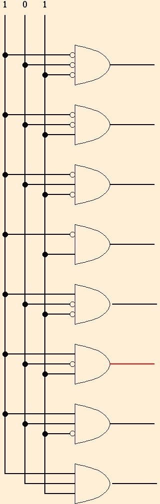
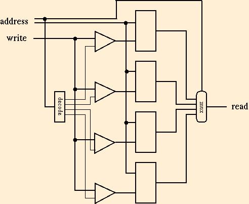
To write a memory location, fan out the value to be written to all
cells, but enable only the addressed cell. Here's a decoder for a
3-bit address:
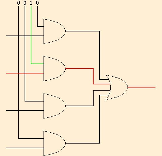
As memories get larger, and spread over more than one silicon chip, both the decoding and the multiplexing get done in more complicated, hierarchical forms.
The essence of building memories is that they can be combined essentially as if they were rectangles in a plane, adding a little bit of extra circuitry for each combining operation. An axb memory is one with a addresses and b bits at each address.
We may also convert an axnb memory to naxb, by using the first logn address bits to multiplex seqments of nb-bit words. The tricky part is writing: the unselected portion of the nb-bit word must be rewritten as it was before.
2's complement vs. other integer encodings.
Selecting a computation step is logically the same as selecting a memory location, but more complicated geometrically because of the irregular structure of the processor. Decoders and multiplexors selectively activate some of the computational datapath, and choose between the results of redundantly activated portions. In particular, the Arithmetic/Logic Unit (ALU) is often organized in bitplanes, much like memory. For logical operations, the bitplanes are independent, but for addition, subtraction, and shift operations there is wiring between adjacent planes. In many cases, it is simplest to let the circuitry calculate all possible operations on the given operands, and use a multiplexor to select the desired one. Integer addition is the most complicated operation that is usually done in this bitplaned/multiplexed fashion. Integer multiplication, and all floating-point operations, usually require some sort of loop, often implemented through microcode.
Integer addition doesn't require a controlled loop, but the need for a carry to propagate down all of the bits of the result slows down the circuit. Lots of tricks are used to improve this, including precharging (since dropping a voltage to ground is usually faster than raising it to VDD), carry-lookahead (calculate the nth carry directly from the input bits at 0 through n), carry-skip (apply carry-lookahead to blocks, ripple between blocks), carry-select (do each 1-bit add both with and without carry, then select the correct answer with a multiplexor)
The control circuitry in the CPU is typically the least regular circuitry in the computer. Functionally, control circuitry implements a finite-state machine (called a ``finite automaton'' in more theoretical classes). Circuitry for finite-state machines can be regularized somewhat by using the form of a combinational transition circuit providing feedback from a state register to itself. The transition circuit may be implemented by a PLA.
Appendix A of the text has a lot more detail on computer arithmetic
From a logical point of view, microcode architecture uses a more primitive computer on the CPU chip to implement the more sophisticated instructions of the real architecture. Microcode programs are stored in read-only memory, but are easier to change during design and production than detailed wiring. Notice that microcoding replaces relatively unstructured control wiring with the highly regular form of memory. They usually manipulate the electronic control signals, rather than values in memory.